
Over the years transistors – the building blocks of digital devices - have become smaller by the day, making devices faster and compact. But this has also meant increased wastage of power. A group of Indian scientists have found a way to address this problem.
Transistors work by acting like electronic switches controlling the flow of current across circuits. The most common type of transistors called MOSFETs (metal–oxide–semiconductor field-effect transistors) cannot switch from ‘on’ to ‘off’ abruptly and thus leak current even after the device is turned off. The smaller the transistors are more power they waste. Tunnel FETs (field-effect transistors) waste much less power but are more suited for low performance devices like watches or notebook computers.
Scientists at the Indian Institute of Science (IISc) at Bengaluru have combined these two different types of transistors into a single device that can easily switch between power-efficient and high performance modes, depending on the need. The device has a special type of metal-semiconductor junction which can be tweaked to make it behave either like a MOSFET or a tunnel FET.
" The device has a special type of metal-semiconductor junction which can be tweaked to make it behave either like a MOSFET or a tunnel FET. "
“MOSFETs typically work like floodgates in a dam – they have a source, a drain, and a gate that controls flow of electrons between the two. When the gate is in the OFF position, there is a large energy barrier which prevents electrons from crossing over. When gate is turned on with voltage, height of the barrier is reduced and electrons can jump over. The smaller the supply voltage to turn the transistor on, more efficient is the device,” explained Dr Navakanta Bhat, head of the Centre for Nano Science and Engineering at IISc who led the research team.
However, he said, bringing down supply voltage for MOSFETs proportionately with transistor size is difficult because of a fundamental design flaw. A factor called subthreshold swing – which determines the minimum gate voltage required for the transistor to switch from on to off – restricts the supply voltage to be not less than 1 volt.
To overcome this, scientists have tried using tunnel FETs in which instead of the height, the width of the electron barrier is reduced to a point where electrons are able to “tunnel” through instead of jumping over it. Tunnel FETs can operate at lower supply voltages but the current flowing when the transistor is on is greatly reduced.
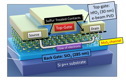
In the present work, researchers designed a hybrid device capable of switching between MOSFET and tunnel FET modes by using two gates instead of one, and a special type of electron barrier created by joining a metal and semiconductor under certain conditions. The dual-gated device, Dr. Bhat said, is able to operate at a voltage lower than possible with conventional MOSFETs, greatly reducing power consumption.
The research results have been published in journal Applied Physics Letters. The team included Dr. Bhat and Shubhadeep Bhattacharjee. (India Science Wire)