Advanced two-dimensional graphene-like materials are proving to be exceptionally useful in miniaturising electronics, with a potential to replacing bulky devices made from silicon or germanium. Because of this, understanding the material’s electrophysical properties before fabricating the device is of prime importance, and hence there is a high demand for such tools.
An international team of interdisciplinary scientists led by researchers from the Indian Institute of Science (IISc), Bengaluru, have developed a computational tool to evaluate the performance of advanced graphene-like two dimensional (2D) materials. It can assess the effects of electron-phonon scattering on current through electronic devices in integrated circuits. By using this code, one can peek into the quantum lattice vibrations of the crystal, pre-evaluate the performance of the advanced material, and check its suitability for a device, before manufacturing them.
The study offers one such model to evaluate the electron-phonon interactions in the material. In a semiconductor, at the quantum level, there exist two systems: the electron-hole charge carriers and another called phonon that originates from the lattice vibrations.
“In the semiconducting channel of a device such as a transistor, electrons/holes carriers transport the charge (and information encoded within the charge) from the input to the output end. The phonons interact with carriers during this transport and create ‘resistance’, which affects the performance such as drive current and speed of operation. Strength of such interaction is material-specific, and thus it is crucial to understand the interaction when we plan to design transistors fabricated with the 2D materials,” explained Dr Santanu Mahapatra, team lead of the study and professor at IISc, while speaking to India Science Wire.
The electron-phonon coupling limited transport is a complex process, and in this study, the low-energy two-band model was used for the computation.
Dr. Santanu Mahapatra and Arnab Kabiraj
" In the semiconducting channel of a device such as a transistor, electrons/holes carriers transport the charge (and information encoded within the charge) from the input to the output end."
The team employed a software tool called VASP to analyse the energy band structure of different materials. They developed the extensive software code by using Hybrid C and MATLAB programming style.
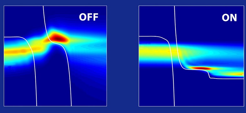
Using the simulated model, the team has demonstrated the performance of a phosphorene based MOSFET (building blocks of ICs). The atomic structure of the material has a web-like distribution where the atoms are patterned in a sequential form (called the armchair format) and also in a zig-zag fashion. They observed that for phosphorene, electron-phonon scattering is more pronounced in the zigzag direction.
Dr Bhaskaran Muralidharan, associate professor, Indian Institute of Technology, Bombay, who was not involved in the study, commented, "this work provides a method to understand the microscopic mechanism of 'backscattering' that impedes the transfer of information in devices.
The study shows potential as a sophisticated tool to know along what direction some 2D materials can actually show minimal scattering, thereby improving the performance of such nanoscale devices."
The research was supported by Department of Science and Technology, and by the Council for Scientific and Industrial Research. The project was carried out under collaboration with CNRS, Marseille (France), which was initiated through Raman-Charpak fellowship program.
The team included Madhuchanda Brahma, Arnab Kabiraj and Santanu Mahapatra from IISc, Bengaluru, and Marc Bescond from the University of Tokyo. The results were published in the Journal of Applied Physics.
India Science Wire