Figure: Light manipulation via exciting the polaritons in GaN nanostructured. By controlling the morphology of the GaN nanostructures, the polariton excitations are tuned in a controlled way.
Gallium Nitride (GaN) is the fundamental building block for Power Electronics. Researchers from Jawaharlal Nehru Centre for Advanced Scientific Research (JNCASR), Bengaluru, an autonomous institute of the Department of Science and Technology, have for the first time demonstrated Infra-Red (IR) light emission and absorption with GaN nanostructures.
For decades, silicon-based MOSFETs (Metal Oxide Semiconductor Field Effect Transistors) have been an integral part of the everyday modern world. It helps convert energy to power. However, owing to the limitations to improving silicon MOSFETs, researchers are searching for alternatives. The use of GaN is on the rise to replace silicon as the backbone of power-switching technology.
Though blue light emission from GaN is not an unfamiliar phenomenon and has been used in LEDs, IR light-matter interactions in GaN have been demonstrated the first time. The researchers utilised a scientific phenomenon called surface polariton excitations in GaN nanostructures, leading to light-matter interactions at IR spectral range.
“Due to ultrabright and stable blue light emission, GaN has emerged as one of the most famous semiconductors of the modern era, useful for light-emitting diodes, power electronics, and optoelectronic applications. Extending GaN’s optical resonance from visible to mid and far-infrared spectral ranges will enable novel applications in many emerging technologies,” researchers write.
Although visible and UV light applications of GaN have already been realised, and LEDs and laser diodes are now commercially available, use of GaN for IR light harvesting or development of GaN-based IR optical elements is still not established.
The new method employed by the scientists to confine and absorb IR light with GaN nanostructures can help develop efficient infrared absorbers, emitters, and modulators that may find several applications including defence and energy development technologies, imaging, sensing, etc.
Gallium Nitride (GaN) is the fundamental building block for Power Electronics. Researchers from Jawaharlal Nehru Centre for Advanced Scientific Research (JNCASR), Bengaluru, an autonomous institute of the Department of Science and Technology, have for the first time demonstrated Infra-Red (IR) light emission and absorption with GaN nanostructures.
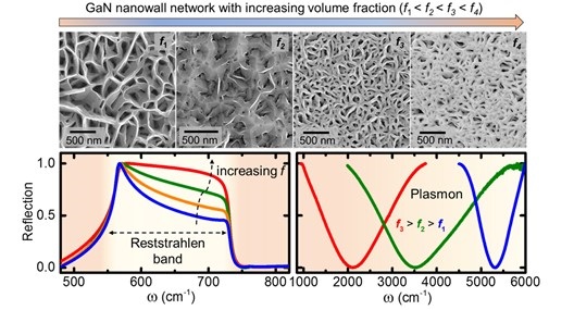
“Here we show hexagonal honeycomb-shaped GaN nanowall networks and vertically standing nanorods exhibiting morphology-dependent Reststrahlen band and plasmon polaritons that could be harnessed for infrared nanophotonics,” researchers explain.
They have utilised a specialised material deposition instrument called molecular beam epitaxy to grow these GaN nanostructures at their International Centre for Materials Science in JNCASR. Their device uses ultra-high vacuum, similar to the conditions of outer space, in order to grow high-quality material nanostructures 100000 times smaller than the width of a human hair.
Polaritons are curious hybrids, being half light and half matter. They are formed when a photon combines with an electronic transition, thus combining the properties of light with those of matter. They find various applications, such as quantum computers, secure high-speed light-based communication (LiFi), solar energy converters, next-generation light sources, and waste-heat converters.
According to the researchers, demonstration of morphology-controlled reststrahlen band and plasmon polaritons make GaN nanostructures attractive for infrared nanophotonics. Nanophotonics finds widespread use in light harvesting, sensing, luminescence, optical switching, and media transmitting technologies.
“Our work demonstrates a novel pathway for utilising GaN in infrared nanophotonic applications. Importantly, we believe that the infrared surface polariton excitations that we have demonstrated could be translated to many other semiconductors as well”, said Dr Bivas Saha, Assistant Professor at the JNCASR.
Silicon is failing to meet the modern demands regarding environmental pollution regulations. GaN can meet the growing needs with better power systems efficiency, performance and system cost.
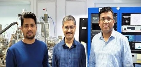
The team of researchers from JNCASR, Bengaluru, comprised Krishna Chand Maurya, Abhijit Chatterjee, Sonnada Math Shivaprasad, and Bivas Saha. The findings of the study have been published in Nano Letters by ACS Publications.
India Science Wire
ISW/SM/GaN/JNCASR/Eng/26/12/2022