In a development that could boost optical or light-based computing, a group of Indian scientists has developed a photodetector device by integrating sheets of nanomaterials with silicon. The device could be used to develop a switch for optical computing and could also make silicon solar cells more efficient.
Computers, at present, use electronic circuits consisting of transistors – tiny devices which act like an on/off switch for streams of electrons. This is called binary switching. In the same way, optical computing works on switches that get activated with light or beams of photons. Developing a photodetector that works with a wide range of light has engaged scientists in recent years.
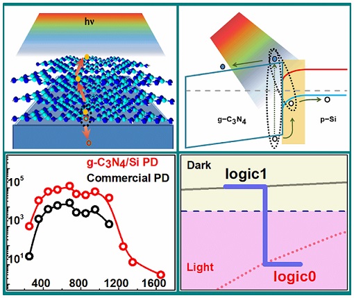
Scientists at the CSIR-National Physical Laboratory (NPL) in New Delhi have now developed a photodetector that can operate over a broadband range of light (250 to 1650 nanometers) and displays binary photoswitching behaviour over a similar range 250 to 1350 nanometers. Such high-performance level for a multifunctional photodetector has been achieved for the first time, researchers have claimed in their study published in journal Advanced Optical Materials.
At the core of the photodetector is a new class of semiconducting material called graphitic carbon-nitride. Scientists at NPL integrated ultrathin nanosheets of graphitic carbon-nitride with silicon. Though graphitic carbon-nitride is projected as next generation material for energy harvesting devices, storage, photo-catalyst and optoelectronic applications, its full understanding and its integration with silicon is in its infancy.
Team of researchers at CSIR-NPL
" Computers, at present, use electronic circuits consisting of transistors – tiny devices which act like an on/off switch for streams of electrons. This is called binary switching. In the same way, optical computing works on switches that get activated with light or beams of photons."
“We have tried to overcome this bottleneck by ultra-thinning graphitic carbon-nitride using a versatile and low-cost technique of ultrasonic exfoliation. The ultrathin graphitic carbon-nitride was then integrated with surface modified silicon substrate via two stage etching process,” explained Dr Prabir Pal and Dr Suraj P. Khanna, who jointly led the research team, while speaking to India Science Wire.
The process involved using ultrasonication to achieve critical structural rearrangement with a high degree of exfoliation in graphitic carbon-nitride nanosheets. This enhanced light absorption capabilities of the material, added Dr Surinder P. Singh ,a member of the research team.
The light absorption was significant over a broad range of spectrum due to reduced dimensionality and large specific area of graphitic carbon-nitride. The overall result was a detector with high photosensitivity as compared to the commercially available counterparts. The device also displayed a novel binary photoswitching (change in current from positive to negative) in response to off/on light illumination. Researchers said the device could be further modified for integration in light-based processors.
“The seamless integration of graphitic carbon-nitride with silicon means it can also be utilized for enhancing the performance of existing energy harvesting devices,” said Dr Khanna.
The research team included Nisha Prakash, Gaurav Kumar, Manjri Singh, Arun Barvat, Prabir Pal, Surinder P. Singh, H. K. Singh, and Suraj P. Khanna. The research work was supported ny NPL, University Grants Commission and Department of Science and Technology (DST) Start-Up Research Grant (Young Scientists) of Science and Engineering Research Board (SERB). (India Science Wire)