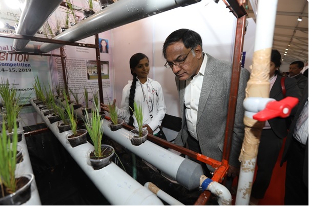
India is a leading player in nanotechnology research globally. To facilitate research in this sector, a national facility for Atom Probe Tomography has been established at the Indian Institute of Technology Madras, in partnership with several other institutes.
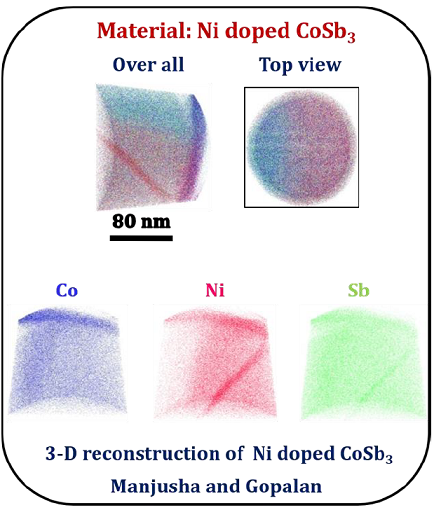
Nanotechnology involves studying materials at the atomic level. Atom Probe Tomography with local electrode is currently the only method that can determine both three-dimensional structure and the chemical composition of a material at an atomic resolution. Before the advent of this technology, transmission electron microscope was used to probe materials, but it can provide information only in two dimensions.
“Local Electrode Atom Probe (LEAP) has an extremely fast acquisition rate of atoms from the sample and can work for a wide range of materials,” explained B S Murty, a scientist at IIT Madras.
In this method, the specimen is first shaped as sharp needle using a focussed beam of gallium ions. When high energy ions strike the sample, atoms eject from its surface. This helps in shaping the sample into a sharp needle. Laser pulses are then applied to the needle-shaped specimen. This strips away the atoms that are present on its tip and converts them into charged ions. These ions hit a detector that can register its position and the time it took to travel from the sample to the detector. These parameters are then used to infer the identity of the ion.
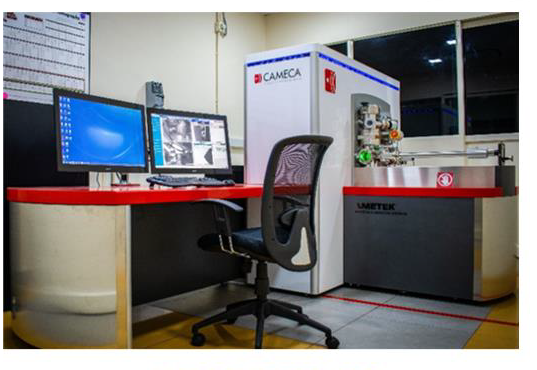
" Local Electrode Atom Probe (LEAP) has an extremely fast acquisition rate of atoms from the sample and can work for a wide range of materials " :B S Murty, a scientist at IIT Madras.
Thus, atom-by-atom, the LEAP microscope can create a three-dimensional image of the sample. This method is particularly useful in determining buried features and interfaces inside a material.
“This is for the first time when eight institution in the country have contributed financially to set up such a platform at a cost of nearly Rupees 40 crores”, Dr Murty told India Science Wire.
The partner institutes include Indian Institutes of Technology at Bombay, Delhi, Kanpur, Kharagpur, Madras and Ropar, and International Advanced Research Centre for Powder Metallurgy and New Materials (Hyderabad), Board of Research in Nuclear Sciences and DST Nano Mission.
Another feature of the new facility is that it is the first remotely operable LEAP in the world. Each of the partner institute have a local workstation that helps scientists to remotely interact with the facility. Using their respective workstation, they can log-in into the system, control experimental parameters, align the specimen, and acquire the data. The workstations have also been configured with full data analysis capabilities.
Apart from materials research, this technique is helpful for research in storage materials, bio-materials, catalytic materials and geochemistry. The facility also houses a Tecnai T12 TEM microscope that produces high-resolution, two-dimensional images, allowing for a wide range application. This facility hopes to cater to the advanced materials characterization needs of Indian research community.
India Science Wire